Your code is clean. Your logic is sound. Yet your embedded system crashes under load, draws too much power, or won’t talk to sensors reliably. You blame the compiler—again. But here’s the hard truth: embedded system hardware design flaws are silently sabotaging your software before it even boots. Most developers treat PCB layout like plumbing—just connect the pipes. That mindset guarantees intermittent bugs, EMI nightmares, and field failures that cost 10x more to fix post-launch.
Why “good enough” hardware ruins embedded projects
Too many teams ship boards wired like breadboards on steroids. Traces meander. Ground planes vanish near high-speed lines. Decoupling caps sit meters (electrically) from ICs. And don’t get me started on mixed-signal isolation.
Here’s the reality: firmware can’t compensate for a starved power rail or crosstalk-induced bit flips. The math is simple—noise margins shrink as clock speeds climb. A layout that “worked” at 8 MHz fails catastrophically at 120 MHz. Yet junior engineers still copy-paste reference designs without understanding parasitic inductance or return current paths.
Worse? Simulation is skipped to “save time.” Guess what—you’ll burn weeks debugging ghost glitches instead.
The step-by-step guide to robust embedded system hardware design
Start with power integrity—not pinouts
Forget GPIO assignments first. Map your power domains early. How many rails? What peak current per rail? Where will switching noise couple into analog sections? Lay solid ground planes before routing a single signal. Use multiple vias for high-current paths—thermal relief pads aren’t optional.
Control impedance like your job depends on it
USB, Ethernet, DDR—all demand controlled impedance. At 50+ MHz, a trace isn’t just copper; it’s a transmission line. Mismatched Z₀ causes reflections that corrupt data. Calculate width/spacing using your stack-up’s εᵣ. Don’t trust online calculators blindly—verify with field solvers.
Decouple smarter, not harder
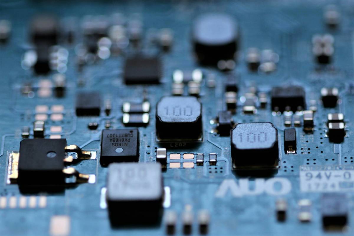
Tossing 100nF caps everywhere is amateur hour. Place 10µF tantalum near the regulator, then 100nF + 1nF ceramic within 5mm of each IC power pin. High-frequency noise needs ultra-low ESL parts—0402 beats 0805 here.
| Design Approach | Time to First Boot | Rework Cycles | Field Failure Rate |
|---|---|---|---|
| Reference Design Copy-Paste | 3–5 days | 2–4 | 8–12% |
| Rigorous Power + Signal Integrity Focus | 7–10 days | 0–1 | <1% |
The industry secret no one talks about
Top-tier firms simulate thermal performance before spinning PCBs. Why? Because a CPU running at 95°C throttles clocks unpredictably—crashing real-time tasks silently. They model airflow, copper weight, and enclosure materials in tools like SimScale or Ansys Icepak. Cost? A few hundred dollars. Savings? Avoiding a $500k recall because units failed in Arizona summers.
And here’s the kicker: they intentionally add test points for power rail ripple—not just JTAG. Monitoring VCC noise during stress tests catches layout issues before certification.
Frequently Asked Questions
What’s the biggest mistake in embedded system hardware design?
Ignoring return current paths. High-speed signals loop back through ground planes—if split by slots or voids, you create EMI antennas.
Do I really need a 4-layer board for simple projects?
Yes, if you use any wireless or >20 MHz clocks. Two signal layers sandwiched between solid power/ground planes suppress noise dramatically.
How critical is component placement?
More than routing. Keep RF sections isolated, place crystals close to MCU pins, and never route digital traces under analog sensors.